Digital Device Overview
In this topic:
Common Parameters
A number of model parameters are common to most of the digital models. These are described below.
Family Parameters
These identify the logic family to which the input and outputs belong. See Analog-Digital Interfaces for more information. Most models have three family parameters:
| Family name | Description |
| in_family | Specifies family for inputs. If omitted, the input family is specified by the FAMILY parameter |
| out_family | Specifies family for outputs. If omitted, the output family is specified by the FAMILY parameter |
| family | Default value for IN_FAMILY and OUT_FAMILY |
VSUPPLY Parameter
The VSUPPLY parameter defines the supply voltage of the device. This controls the following:
- Analog output voltage levels when connected to an analog signal. The voltage levels are determined by the D-A bridge device connected to interface to the analog signal. However, the VSUPPLY parameter, if present, will modify the D-A bridge's output levels by scaling them by a value of VSUPPLY/VSUPPLY_NOMINAL. VSUPPLY_NOMINAL is a bridge parameter and defines the expected supply voltage.
- Input analog thresholds. The VSUPPLY parameter is used to scale the analog input thresholds. The thresholds themselves are determined by the A-D bridge model used to interconnect the digital input to the analog signal. The VSUPPLY parameter will scale these relative to the VSUPPLY_NOMINAL parameter of the A-D bridge
- High state digital plot value. When plotting pure digital signals, VSUPPLY determines the value given to the high state
Further information: Analog to Digital Interfaces
Output Parameters
| Parameter name | Description |
| out_res_pos | This is used to calculate loading delay for positive transitions. It has dimensions of Ohms so is referred to as a resistance. The additional loading delay is calculated by multiplying out_res_pos by the total capacitative load detected on the node to which the output connects. |
| out_res_neg | Same as out_res_pos for negative transitions. |
| out_res | Value for out_res_pos and out_res_neg if not specified or supported |
| min_sink | Used to calculate static loading effects. This is the current that the device is able to sink. Current flowing out of the pin is positive so this parameter is usually negative. If the total sink load current is arithmetically smaller (i.e. more negative) than this parameter then the output will be forced to an UNKNOWN state. This is used to implement fan out limitations in bipolar logic. |
| max_source | Used to calculate static loading effects. This is the current that the device is able to source. Current flowing out of the pin is positive. If the total source load current is larger than this parameter then the output will be forced to an UNKNOWN state. This is used to implement fan out limitations in bipolar logic. |
Input Parameters
| Parameter name | Description |
| sink_current | Current that the input sinks. Positive current flows into the device so this parameter is usually negative. The total of all the input sink currents are added together when a node is in the logic '0' state. If the total sink load current is arithmetically smaller (i.e. more negative) than the MIN_SINK parameter of the device driving the node, then it will be forced to an UNKNOWN state. This is used to implement fan out limitations in bipolar logic. |
| source_current | Current that the input sources. Positive current flows into the device. The total of all the input source currents are added together when a node is in the logic '1' state. If the total source load current is larger than the MAX_SOURCE parameter of the device driving the node, then it will be forced to an UNKNOWN state. This is used to implement fan out limitations in bipolar logic. |
Delays
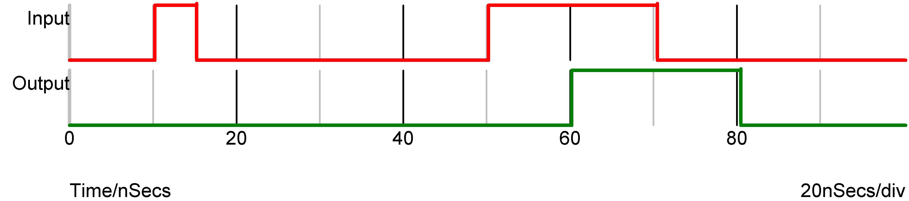
Most digital devices have at least one model parameter that specifies a time delay. Unless otherwise noted, all delays are inertial. This means that glitches shorter than the delay time will be swallowed and not passed on. For example, the following waveforms show the input and output of a gate that has a propagation delay of 10nS. The first pulse is only 5nS so does not appear at the output. The second pulse is 20nS so therefore is present at the output delayed by 10nS.
The Buffer device has an optional stored delay (also known as transport delay) parameter that makes possible the specification of pure delays.
| ◄ Device List | Gates ▶ |