Flip-Flops and Latches
In this topic:
D-type Flip Flop

Netlist entry
Axxxx data clk set reset out nout model_name
Connection details
| Name | Description | Flow | Type |
| data | Input data | in | d |
| clk | Clock | in | d |
| set | Asynchronous set | in | d |
| reset | Asynchronous reset | in | d |
| out | Data output | out | d |
| nout | Inverted data output | out | d |
Model format
.MODEL model_name d_dff parameters
Model parameters
| Name | Description | Type | Default | Limits | ||||||
| clk_delay | Delay from clk | real | 1nS | 1e-12 ???MATH???- \infty???MATH??? | ||||||
| set_delay | Delay from set | real | 1nS | 1e-12 ???MATH???- \infty???MATH??? | ||||||
| reset_delay | Delay from reset | real | 1nS | 1e-12 ???MATH???- \infty???MATH??? | ||||||
| ic |
Output initial state
|
integer | 0 | 0 - 2 | ||||||
| rise_delay | Rise delay | real | 1nS | 1e-12 ???MATH???- \infty???MATH??? | ||||||
| fall_delay | Fall delay | real | 1nS | 1e-12 ???MATH???- \infty???MATH??? | ||||||
| data_load | Data load value (F) | real | 1pF | none | ||||||
| clk_load | Clk load value (F) | real | 1pF | none | ||||||
| set_load | Set load value (F) | real | 1pF | none | ||||||
| reset_load | Reset load value (F) | real | 1pF | none | ||||||
| family | See Family parameters | string | UNIV | none | ||||||
| in_family | See Family parameters | string | UNIV | none | ||||||
| out_family | See Family parameters | string | UNIV | none | ||||||
| out_res | See Output Parameters | real | 100 | ???MATH???0 - \infty???MATH??? | ||||||
| out_res_pos | See Output Parameters | real | out_res | ???MATH???0 - \infty???MATH??? | ||||||
| out_res_neg | See Output Parameters | out_res | ???MATH???0 - \infty???MATH??? | |||||||
| min_sink | See Output Parameters | real | -0.001 | none | ||||||
| max_source | See Output Parameters | real | 0.001 | none | ||||||
| sink_current | See Input Parameters | real | 0 | none | ||||||
| source_current | See Input Parameters | real | 0 | none | ||||||
| vsupply | See vsupply Parameter | real | 5 | none |
Device Operation
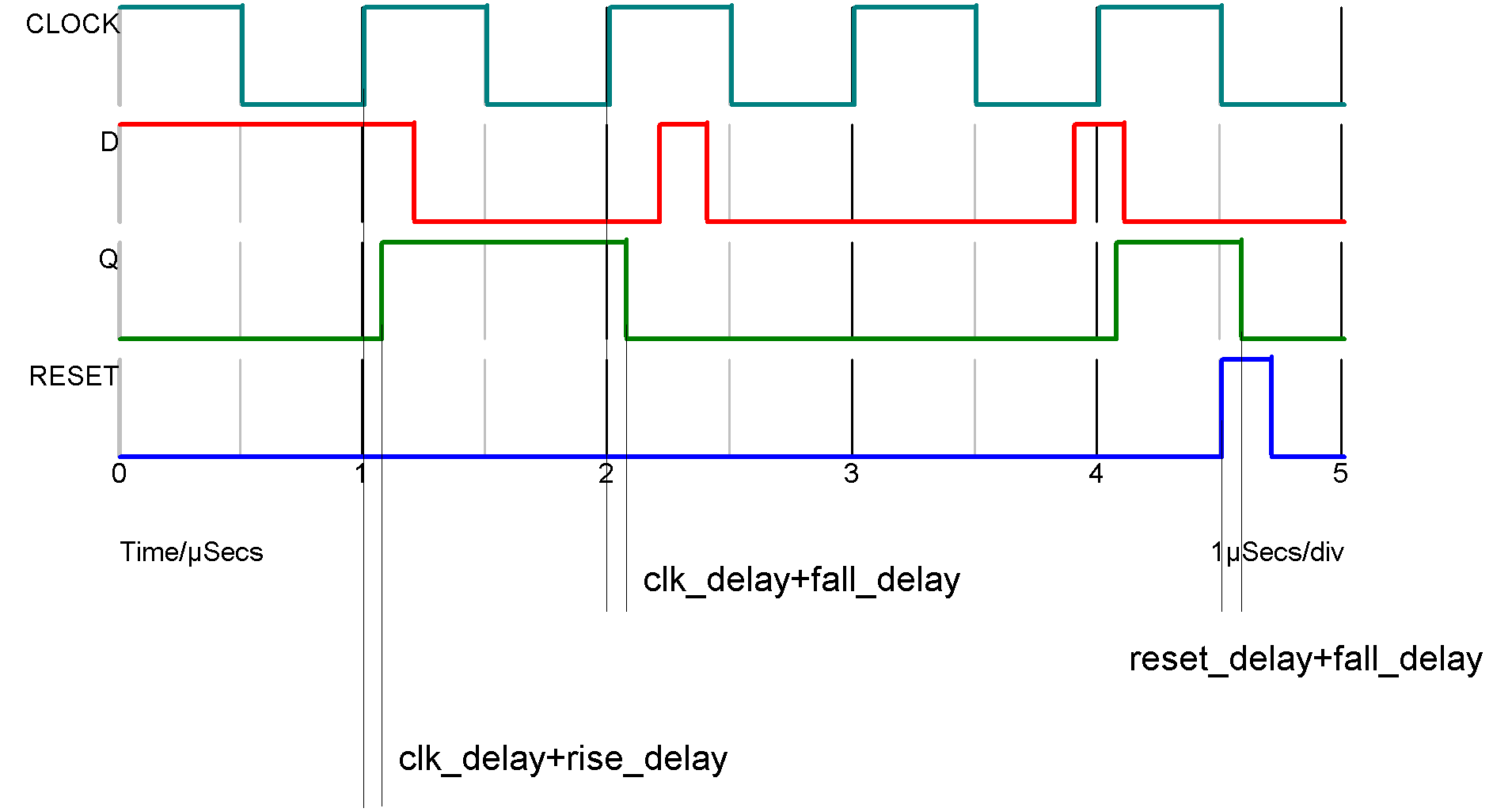
This device has been superseded by Universal Flip-flop using model parameter "type=D".
The device is an edge triggered D-type flip flop with active high asynchronous set and reset. The operation of the device is illustrated by the following diagram:
D-type Latch

Netlist entry
Axxxx data enable set reset out nout model_name
Connection details
| Name | Description | Flow | Type |
| data | Input data | in | d |
| enable | Enable | in | d |
| set | Asynchronous set | in | d |
| reset | Asynchronous reset | in | d |
| out | Data output | out | d |
| nout | Inverted data output | out | d |
Model format
.MODEL model_name d_dlatch parameters
Model parameters
| Name | Description | Type | Default | Limits | ||||||
| data_delay | Delay from data | real | 1nS | 1e-12 ???MATH???- \infty???MATH??? | ||||||
| enable_delay | Delay from enable | real | 1nS | 1e-12 ???MATH???- \infty???MATH??? | ||||||
| set_delay | Delay from set | real | 1nS | 1e-12 ???MATH???- \infty???MATH??? | ||||||
| reset_delay | Delay from reset | real | 1nS | 1e-12 ???MATH???- \infty???MATH??? | ||||||
| ic |
Output initial state
|
integer | 0 | 0 - 2 | ||||||
| rise_delay | Rise delay | real | 1nS | 1e-12 ???MATH???- \infty???MATH??? | ||||||
| fall_delay | Fall delay | real | 1nS | 1e-12 ???MATH???- \infty???MATH??? | ||||||
| data_load | Data load value (F) | real | 1pF | none | ||||||
| enable_load | Enable load value (F) | real | 1pF | none | ||||||
| set_load | Set load value (F) | real | 1pF | none | ||||||
| reset_load | Reset load value (F) | real | 1pF | none | ||||||
| family | See Family parameters | string | UNIV | none | ||||||
| in_family | See Family parameters | string | UNIV | none | ||||||
| out_family | See Family parameters | string | UNIV | none | ||||||
| out_res | See Output Parameters | real | 100 | ???MATH???0 - \infty???MATH??? | ||||||
| out_res_pos | See Output Parameters | real | out_res | ???MATH???0 - \infty???MATH??? | ||||||
| out_res_neg | See Output Parameters | out_res | ???MATH???0 - \infty???MATH??? | |||||||
| min_sink | See Output Parameters | real | -0.001 | none | ||||||
| max_source | See Output Parameters | real | 0.001 | none | ||||||
| sink_current | See Input Parameters | real | 0 | none | ||||||
| source_current | See Input Parameters | real | 0 | none | ||||||
| vsupply | See vsupply Parameter | real | 5 | none |
Device Operation
This device has now been superseded by D-type Latch (New).
The device is a level triggered latch with a single data input, complimentary outputs and active high asynchronous set and reset. The operation of the device is illustrated in the following diagram:

The asynchronous inputs (set and reset) override the action of the enable and data lines.
D-type Latch (New)
This device has the same functionality as the older D-type Latch (D-type Latch) but this newer version implements signal delays in a manner that is more representative of real devices and is recommended for new designs. The generic D-type latch available in the schematic editor uses this device.
Netlist entry
Axxxx data enable set reset out nout model_name
Connection details
| Name | Description | Flow | Type |
| data | Input data | in | d |
| enable | Enable | in | d |
| set | Asynchronous set | in | d |
| reset | Asynchronous reset | in | d |
| out | Data output | out | d |
| nout | Inverted data output | out | d |
Model format
.MODEL model_name d_latch parameters
Model parameters
| Name | Description | Type | Default | Limits | ||||||
| ic |
Output initial state
|
integer | 0 | 0 - 2 | ||||||
| enable_delay | Enable delay | real | 1n | 1e-15 ???MATH???- \infty???MATH??? | ||||||
| data_delay | Data delay | real | 1n | 1e-15 ???MATH???- \infty???MATH??? | ||||||
| async_delay | Set/reset delay | real | 1n | 1e-15 ???MATH???- \infty???MATH??? | ||||||
| rise_delay | Rise delay | real | 1nS | 0 ???MATH???- \infty???MATH??? | ||||||
| fall_delay | Fall delay | real | 1nS | 0 ???MATH???- \infty???MATH??? | ||||||
| async_polarity | 1: active high, 0: active low | integer | 1 | none | ||||||
| enable_polarity | 1: high, 0: low | integer | 1 | none | ||||||
| input_load | Default load for all inputs unless overridden (F) | real | 1pF | none | ||||||
| data_load | Data load value (F) | real | 1pF | none | ||||||
| enable_load | Enable load value (F) | real | 1pF | none | ||||||
| set_load | Set load value (F) | real | 1pF | none | ||||||
| reset_load | Reset load value (F) | real | 1pF | none | ||||||
| family | See Family parameters | string | UNIV | none | ||||||
| in_family | See Family parameters | string | UNIV | none | ||||||
| out_family | See Family parameters | string | UNIV | none | ||||||
| out_res | See Output Parameters | real | 100 | ???MATH???0 - \infty???MATH??? | ||||||
| out_res_pos | See Output Parameters | real | out_res | ???MATH???0 - \infty???MATH??? | ||||||
| out_res_neg | See Output Parameters | out_res | ???MATH???0 - \infty???MATH??? | |||||||
| min_sink | See Output Parameters | real | -0.001 | none | ||||||
| max_source | See Output Parameters | real | 0.001 | none | ||||||
| sink_current | See Input Parameters | real | 0 | none | ||||||
| source_current | See Input Parameters | real | 0 | none | ||||||
| vsupply | See vsupply Parameter | real | 5 | none |
Device Operation
The device is a level triggered latch with a single data input, complimentary outputs and active high asynchronous set and reset. The operation of the device is illustrated in the following diagram:
Note that any signal on the enable, set, reset or data that is shorter than the associated delay time will not be actioned. So for example, if the enable_delay parameter is set to 10ns, a 9.9ns pulse on the enable input will not enable the latch whereas a 10.1ns pulse will enable the latch. This behaviour is the important difference between this device and the older D-type latch.
The asynchronous inputs (set and reset) override the action of the enable and data lines.
JK Flip Flop
Netlist entry
Axxxx j k clk set reset out nout model_name
Connection details
| Name | Description | Flow | Type |
| j | J input | in | d |
| k | K input | in | d |
| clk | Clock | in | d |
| set | Asynchronous set | in | d |
| reset | Asynchronous reset | in | d |
| out | Data output | out | d |
| nout | Inverted data output | out | d |
Model format
.MODEL model_name d_jkff parameters
Model parameters
| Name | Description | Type | Default | Limits | |
| clk_delay | Delay from clk | real | 1nS | 1e-12 ???MATH???- \infty???MATH??? | |
| set_delay | Delay from set | real | 1nS | 1e-12 ???MATH???0 - \infty???MATH??? | |
| reset_delay | Delay from reset | real | 1nS | 1e-12 ???MATH???0 - \infty???MATH??? | |
| ic | Output initial state | integer | 0 | ???MATH???0 - 2???MATH??? | |
| rise_delay | Rise delay | real | 1nS | 1e-12 ???MATH???0 - \infty???MATH??? | |
| fall_delay | Fall delay | real | 1nS | 1e-12 ???MATH???0 - \infty???MATH??? | |
| jk_load | J,k load values (F) | real | 1pF | none | |
| clk_load | Clk load value (F) | real | 1pF | none | |
| set_load | Set load value (F) | real | 1pF | none | |
| reset_load | Reset load value (F) | real | 1pF | none | |
| family | See Family parameters | string | UNIV | none | |
| in_family | See Family parameters | string | UNIV | none | |
| out_family | See Family parameters | string | UNIV | none | |
| out_res | See Output Parameters | real | 100 | ???MATH???0 - \infty???MATH??? | |
| out_res_pos | See Output Parameters | real | out_res | ???MATH???0 - \infty???MATH??? | |
| out_res_neg | See Output Parameters | out_res | ???MATH???0 - \infty???MATH??? | ||
| min_sink | See Output Parameters | real | -0.001 | none | |
| max_source | See Output Parameters | real | 0.001 | none | |
| sink_current | See Input Parameters | real | 0 | none | |
| source_current | See Input Parameters | real | 0 | none | |
| vsupply | See vsupply Parameter | real | 5 | none |
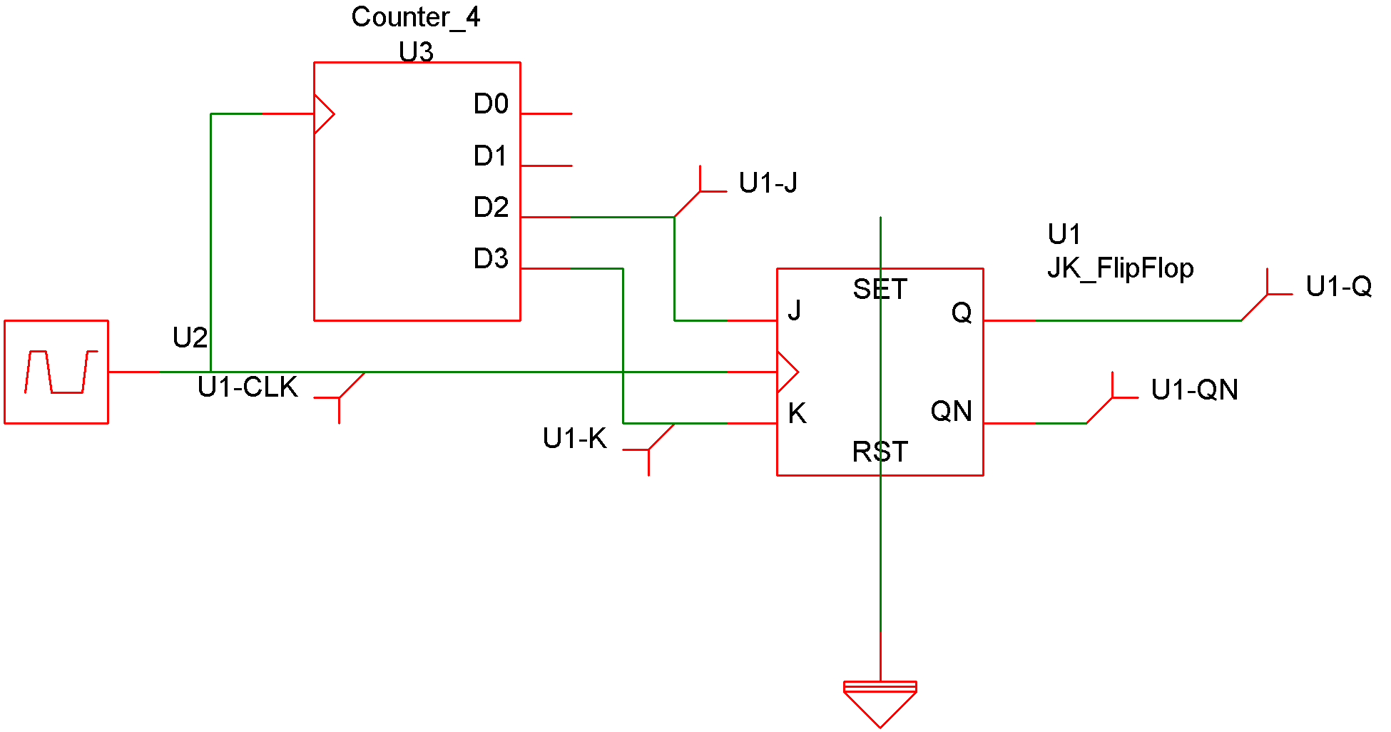
Device Operation
This device has been superseded by Universal Flip-flop using model parameter "type=JK".
The following circuit and graph illustrate the operation of this device:
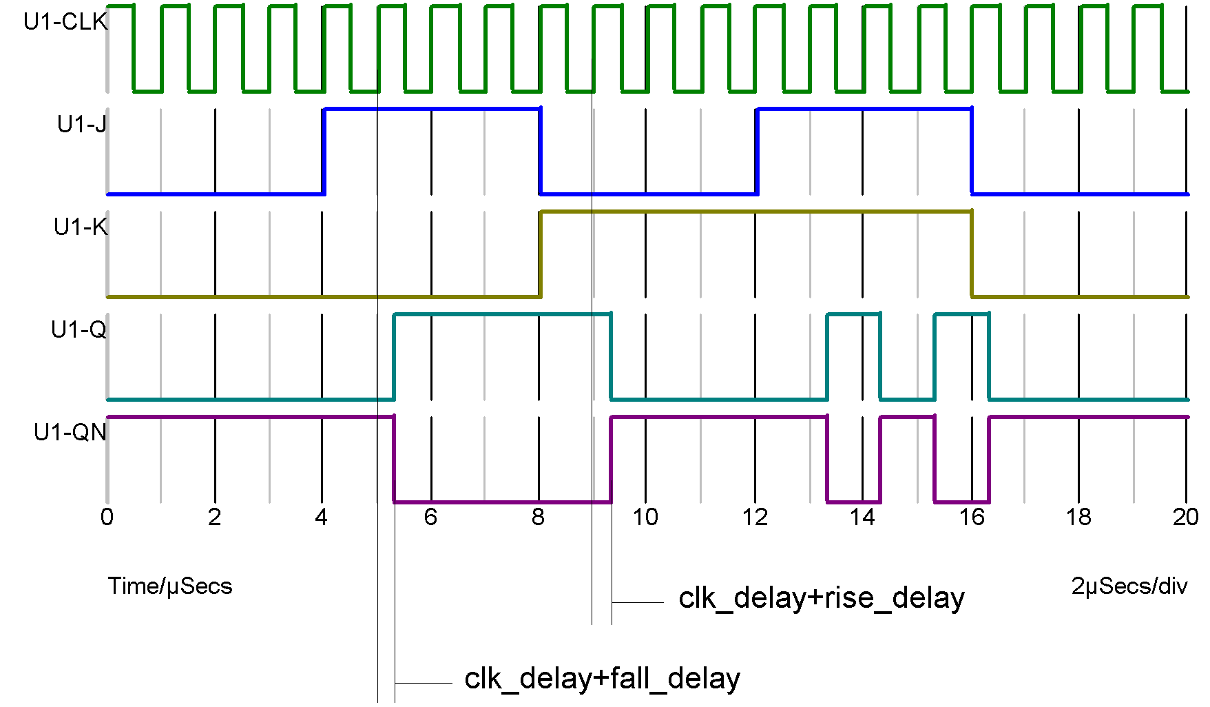
The following table describes the operation of the device when both inputs are at known states: The output can only change on a positive edge of the clock.
| J input | K input | Output |
| 0 | 0 | No change |
| 0 | 1 | 0 |
| 1 | 0 | 1 |
| 1 | 1 | toggle |
| J input | K input | old output | new output |
| 0 | 0 | 0 | 0 |
| 0 | 0 | 1 | 1 |
| 0 | 0 | X | X |
| 0 | 1 | 0 | 0 |
| 0 | 1 | 1 | 0 |
| 0 | 1 | X | 0 |
| 0 | X | 0 | 0 |
| 0 | X | 1 | X |
| 0 | X | X | X |
| 1 | 0 | 0 | 1 |
| 1 | 0 | 1 | 1 |
| 1 | 0 | X | 1 |
| 1 | 1 | 0 | 1 |
| 1 | 1 | 1 | 0 |
| 1 | 1 | X | X |
| 1 | X | 0 | 1 |
| 1 | X | 1 | X |
| 1 | X | X | X |
| X | 0 | 0 | X |
| X | 0 | 1 | 1 |
| X | 0 | X | X |
| X | 1 | 0 | X |
| X | 1 | 1' | 0 |
| X | 1 | X | X |
| X | X | 0 | X |
| X | X | 1 | X |
| X | X | X | X |
Set-Reset Flip-Flop
Netlist entry
Axxxx s r clk set reset out nout model_name
Connection details
| Name | Description | Flow | Type | |
| s | S input | in | d | |
| r | R input | in | d | |
| clk | Clock | in | d | |
| set | Asynchronous set | in | d | |
| reset | Asynchronous reset | in | d | |
| out | Data output | out | d | |
| nout | Inverted data output | out | d |
Model format
.MODEL model_name d_srff parameters
Model parameters
| Name | Description | Type | Default | Limits | |
| clk_delay | Delay from clk | real | 1nS | ???MATH???1\text{e}^{-12} - \infty???MATH??? | |
| set_delay | Delay from set | real | 1nS | ???MATH???1\text{e}^{-12} - \infty???MATH??? | |
| reset_delay | Delay from reset | real | 1nS | ???MATH???1\text{e}^{-12} - \infty???MATH??? | |
| ic | Output initial state | integer | 0 | 0 - 2 | |
| rise_delay | Rise delay | real | 1nS | ???MATH???1\text{e}^{-12} - \infty???MATH??? | |
| fall_delay | Fall delay | real | 1nS | ???MATH???1\text{e}^{-12} - \infty???MATH??? | |
| sr_load | S,r load values (F) | real | 1pF | none | |
| clk_load | Clk load value (F) | real | 1pF | none | |
| set_load | Set load value (F) | real | 1pF | none | |
| reset_load | Reset load value (F) | real | 1pF | none | |
| family | See Family parameters | string | UNIV | none | |
| in_family | See Family parameters | string | UNIV | none | |
| out_family | See Family parameters | string | UNIV | none | |
| out_res | See Output Parameters | real | 100 | ???MATH???0 - \infty???MATH??? | |
| out_res_pos | See Output Parameters | real | out_res | ???MATH???0 - \infty???MATH??? | |
| out_res_neg | See Output Parameters | real | out_res | ???MATH???0 - \infty???MATH??? | |
| open_c | Open collector output | boolean | FALSE | none | |
| min_sink | See Output Parameters | real | -0.001 | none | |
| max_source | See Output Parameters | real | 0.001 | none | |
| sink_current | See Input Parameters | real | 0 | none | |
| source_current | See Input Parameters | real | 0 | none | |
| vsupply | See vsupply Parameter | real | 5 | none |
Device Operation
This device has been superseded by Universal Flip-flop using model parameter "type=SR".
The SR flip flop is similar to a JK flip flop except that the output is UNKNOWN when both S and R inputs are high. In a JK the output toggles in the same circumstances.
The following table describes the operation of the device when both inputs are at known states: The output can only change on a positive edge on the clock.
| S input | R input | Output |
| 0 | 0 | No change |
| 0 | 1 | 0 |
| 1 | 0 | 1 |
| 1 | 1 | UNKNOWN |
| S input | R input | old output | new output |
| 0 | 0 | 0 | 0 |
| 0 | 0 | 1 | 1 |
| 0 | 0 | X | X |
| 0 | 1 | 0 | 0 |
| 0 | 1 | 1 | 0 |
| 0 | 1 | X | 0 |
| 0 | X | 0 | 0 |
| 0 | X | 1 | X |
| 0 | X | X | X |
| 1 | 0 | 0 | 1 |
| 1 | 0 | 1 | 1 |
| 1 | 0 | X | 1 |
| 1 | 1 | 0 | X |
| 1 | 1 | 1 | X |
| 1 | 1 | X | X |
| 1 | X | 0 | X |
| 1 | X | 1 | X |
| 1 | X | X | X |
| X | 0 | 0 | X |
| X | 0 | 1 | 1 |
| X | 0 | X | X |
| X | 1 | 0 | X |
| X | 1 | 1' | X |
| X | 1 | X | X |
| X | X | 0 | X |
| X | X | 1 | X |
| X | X | X | X |
SR Latch
Netlist entry
Axxxx s r enable set reset out nout model_name
Connection details
| Name | Description | Flow | Type |
| s | S input | in | d |
| r | R input | in | d |
| enable | Enable | in | d |
| set | Asynchronous set | in | d |
| reset | Asynchronous reset | in | d |
| out | Data output | out | d |
| nout | Inverted data output | out | d |
Model format
.MODEL model_name d_srlatch parameters
Model parameters
| Name | Description | Type | Default | Limits | |
| sr_delay | Delay from s or r input change | real | 1nS | ???MATH???1\text{e}^{-12} - \infty???MATH??? | |
| enable_delay | Delay from clk | real | 1nS | ???MATH???1\text{e}^{-12} - \infty???MATH??? | |
| set_delay | Delay from set | real | 1nS | ???MATH???1\text{e}^{-12} - \infty???MATH??? | |
| reset_delay | Delay from reset | real | 1nS | ???MATH???1\text{e}^{-12} - \infty???MATH??? | |
| ic | Output initial state | integer | 0 | 0 - 2 | |
| rise_delay | Rise delay | real | 1nS | ???MATH???1\text{e}^{-12} - \infty???MATH??? | |
| fall_delay | Fall delay | real | 1nS | ???MATH???1\text{e}^{-12} - \infty???MATH??? | |
| sr_load | S & r load values (F) | real | 1pF | none | |
| enable_load | Clk load value (F) | real | 1pF | none | |
| set_load | Set load value (F) | real | 1pF | none | |
| reset_load | Reset load value (F) | real | 1pF | none | |
| family | See Family parameters | string | UNIV | none | |
| in_family | See Family parameters | string | UNIV | none | |
| out_family | See Family parameters | string | UNIV | none | |
| out_res | See Output Parameters | real | 100 | ???MATH???0 - \infty???MATH??? | |
| out_res_pos | See Output Parameters | real | out_res | ???MATH???0 - \infty???MATH??? | |
| out_res_neg | See Output Parameters | real | out_res | ???MATH???0 - \infty???MATH??? | |
| min_sink | See Output Parameters | real | -0.001 | none | |
| max_source | See Output Parameters | real | 0.001 | none | |
| sink_current | See Input Parameters | real | 0 | none | |
| source_current | See Input Parameters | real | 0 | none | |
| vsupply | See vsupply Parameter | real | 5 | none |
Device Operation
This device is identical to the SR flip flop except that it is level not edge triggered. That is the output may change whenever the enable input is high.
Toggle Flip Flop
Netlist entry
Axxxx t clk set reset out nout model_name
Connection details
| Name | Description | Flow | Type |
| t | Toggle input | in | d |
| clk | Clock | in | d |
| set | Asynchronous set | in | d |
| reset | Asynchronous reset | in | d |
| out | Data output | out | d |
| nout | Inverted data output | out | d |
Model format
.MODEL model_name d_tff parameters
Model parameters
| Name | Description | Type | Default | Limits | |
| clk_delay | Delay from clk | real | 1nS | ???MATH???1\text{e}^{-12} - \infty???MATH??? | |
| set_delay | Delay from set | real | 1nS | ???MATH???1\text{e}^{-12} - \infty???MATH??? | |
| reset_delay | Delay from reset | real | 1nS | ???MATH???1\text{e}^{-12} - \infty???MATH??? | |
| ic | Output initial state | integer | 0 | 0 - 2 | |
| rise_delay | Rise delay | real | 1nS | ???MATH???1\text{e}^{-12} - \infty???MATH??? | |
| fall_delay | Fall delay | real | 1nS | ???MATH???1\text{e}^{-12} - \infty???MATH??? | |
| t_load | Toggle load value (F) | real | 1pF | none | |
| clk_load | Clk load value (F) | real | 1pF | none | |
| set_load | Set load value (F) | real | 1pF | none | |
| reset_load | Reset load value (F) | real | 1pF | none | |
| family | See Family parameters | string | UNIV | none | |
| in_family | See Family parameters | string | UNIV | none | |
| out_family | See Family parameters | string | UNIV | none | |
| out_res | See Output Parameters | real | 100 | ???MATH???0 - \infty???MATH??? | |
| out_res_pos | See Output Parameters | real | out_res | ???MATH???0 - \infty???MATH??? | |
| out_res_neg | See Output Parameters | real | out_res | ???MATH???0 - \infty???MATH??? | |
| min_sink | See Output Parameters | real | -0.001 | none | |
| max_source | See Output Parameters | real | 0.001 | none | |
| sink_current | See Input Parameters | real | 0 | none | |
| source_current | See Input Parameters | real | 0 | none | |
| vsupply | See vsupply Parameter | real | 5 | none |
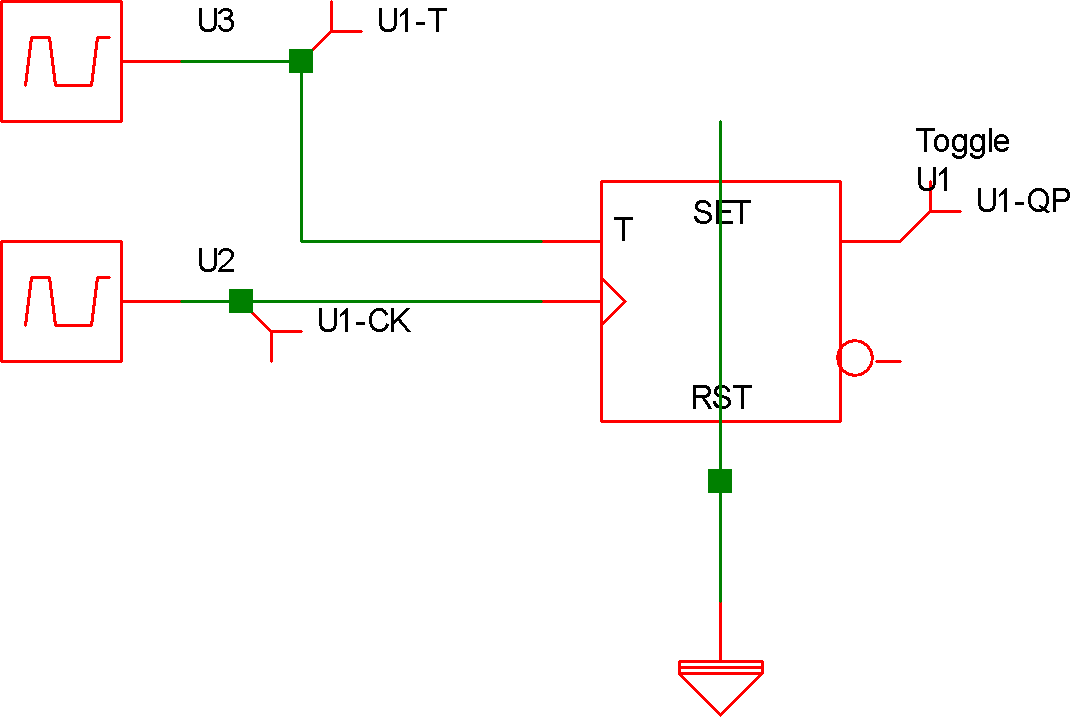
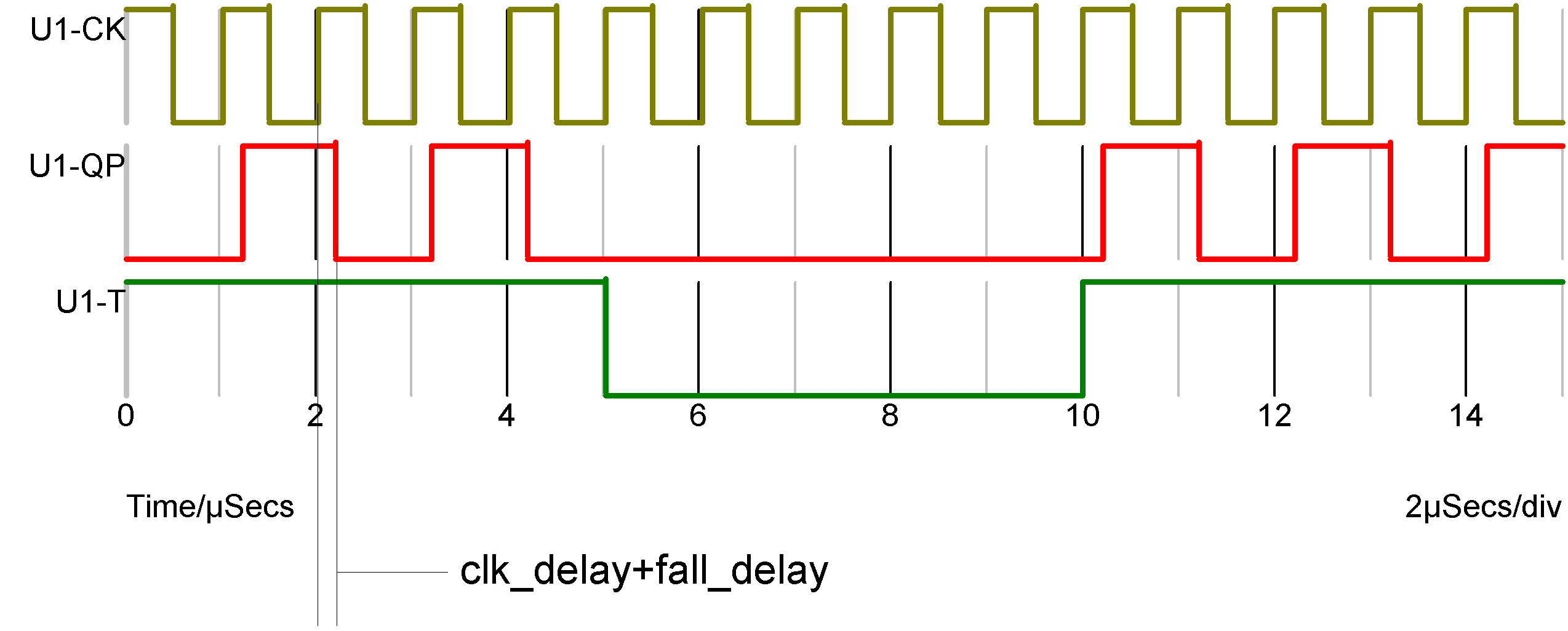
Device Operation
This device has been superseded by Universal Flip-flop using model parameter "type=T".
The operation of the toggle flip flop is illustrated by the following diagrams. When the T input is high, the output toggles on each rising edge of the clock. If the T input is UNKNOWN the output will be UNKNOWN.
Universal Flip-flop
Overview
The universal flip-flop is a general purpose edge-triggered device which can be configured in one of four types. These are D-type, JK, Toggle and SR. The device has more timing control parameters than the older dedicated types and it is recommended that this device is used for all new designs.
Netlist entry
Axxxx in out model_name
Connection details
| Name | Description | Flow | Type |
| data | Data input 1 or 2 pins | in | d, vector |
| clk | Clock in | in | d |
| set | Asynchronous set | in | d |
| reset | Asynchronous reset | in | d |
| out | Output | out | d |
| nout | Inverted Output | out | d |
Model format
.MODEL model_name d_flipflop parameters
Model parameters
| Name | Description | Type | Default | Limits | |
| type | Flip flop type: D, T, JK or RS | string | D | ||
| clk_delay | Clock delay | real | 1ns | 1e-15 ???MATH???- \infty???MATH??? | |
| async_delay | Set/reset delay | real | 1ns | 1e-15 ???MATH???- \infty???MATH??? | |
| rise_delay | Rise delay | real | 0s | 0 ???MATH???- \infty???MATH??? | |
| fall_delay | Fall delay | real | 0s | 0 ???MATH???- \infty???MATH??? | |
| setup_time | Setup time | real | 1ns | ||
| hold_time | Hold time | real | 0s | 0 ???MATH???- \infty???MATH??? | |
| min_clock | Minimum clock width | real | 1ns | 1e-15 ???MATH???- \infty???MATH??? | |
| min_async | Minimum set/reset pulse width | real | 1ns | 1e-15 ???MATH???- \infty???MATH??? | |
| rem_time | Removal time | real | 1ns | 0 ???MATH???- \infty???MATH??? | |
| ic | Initial condition | integer | not applied | 0,1,2 | |
| data_load | Input load | real | 1pF | ||
| clk_load | Clock load | real | 1pF | ||
| set_load | Set load | real | 1pF | ||
| reset_load | Reset load | real | 1pF | ||
| clock_edge_polarity | Clock edge polarity, 1: rising, 0: falling | integer | 1 (rising) | ||
| async_polarity | Set/reset polarity, 1: active high, 0: active low | integer | 1 (active high) | ||
| See Family parameters | string | UNIV | none | ||
| in_family | See Family parameters | string | UNIV | none | |
| out_family | See Family parameters | string | UNIV | none | |
| out_res | See Output Parameters | real | 100 | ???MATH???0 - \infty???MATH??? | |
| out_res_pos | See Output Parameters | real | out_res | ???MATH???0 - \infty???MATH??? | |
| out_res_neg | See Output Parameters | out_res | ???MATH???0 - \infty???MATH??? | ||
| min_sink | See Output Parameters | real | -0.001 | none | |
| max_source | See Output Parameters | real | 0.001 | none | |
| sink_current | See Input Parameters | real | 0 | none | |
| source_current | See Input Parameters | real | 0 | none | |
| vsupply | See vsupply Parameter | real | 5 | none |
Model Parameter Notes
- Total delay from clock edge to output = clk_delay + rise_delay for a 0-1 output transistion and clk_delay + fall_delay for a 1-0 transition
- Total delay from set or reset to output = async_delay + rise_delay for a 0-1 output transistion and clk_delay + fall_delay for a 1-0 transition
- setup_time can be negative but must satisfy setup_time + min_clock >0
- hold_time must satisfy hold_time - min_clock < 0
- Total clock delay must be greater than or equal to min_clock. That is clk_delay + min(rise_delay, fall_delay) >= min_clock
- Total set/reset delay must be greater than or equal to min_async. That is async_delay + min(rise_delay, fall_delay) >= min_async
- The ic parameter can take three possible values: 0: ZERO state, 1: ONE state, 2: UNKNOWN state
Timings
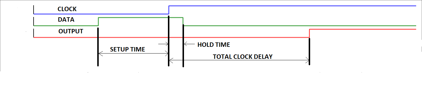 |
Setup and Hold Time |
The diagram above illustrates setup time, hold time and total clock delay. The data input must not change between the setup time before the clock edge to the hold time after the clock edge in order for the data value to be clocked. If this condition is violated the flip-flop will not change state.
 |
Asynchronous Set/Reset Timings |
The diagram above illustrates the aynchronous set/reset timing and its interaction with clock timing. The set and reset signals must be inactive prior to the clock edge, the margin allowed being the removal time (rem_time parameter). If this condition is violated, the subsequent clock edge will be inactive but the set/reset will be successful as long as the minimum pulse width condition is satisfied.
Operation
This device implements four types of edge triggered flip-flop, namely D, T (toggle), J-K and S-R. The type of flip-flop is controlled by the type parameter.
Operation - D-type
On the active clock edge the state of the flip flop acquires the state of the single D input provided the setup and hold times are met. If the D input has an UNKNOWN state, the flip-flop state will also acquire an UNKNOWN state.
Operation - T toggle Flip-Flop
If the single T input is at a logic ONE, the state of the flip-flop inverts on the active clock edge. If the input is at a logic zero, the state remains unchanged.
Operation - J-K Flip-Flop
The J-K flip flop has two inputs. The operation is defined by the following table:
| J input | K input | Output |
| 0 | 0 | No change |
| 0 | 1 | 0 |
| 1 | 0 | 1 |
| 1 | 1 | toggle |
The above table describes the operation for the normal situation when both inputs are in known (ZERO or ONE) states. The complete table including also UNKNOWN states is shown below. In some cases a known state can be clocked even if one of the inputs is unknown.
| J input | K input | old output | new output |
| 0 | 0 | 0 | 0 |
| 0 | 0 | 1 | 1 |
| 0 | 0 | X | X |
| 0 | 1 | 0 | 0 |
| 0 | 1 | 1 | 0 |
| 0 | 1 | X | 0 |
| 0 | X | 0 | 0 |
| 0 | X | 1 | X |
| 0 | X | X | X |
| 1 | 0 | 0 | 1 |
| 1 | 0 | 1 | 1 |
| 1 | 0 | X | 1 |
| 1 | 1 | 0 | 1 |
| 1 | 1 | 1 | 0 |
| 1 | 1 | X | X |
| 1 | X | 0 | 1 |
| 1 | X | 1 | X |
| 1 | X | X | X |
| X | 0 | 0 | X |
| X | 0 | 1 | 1 |
| X | 0 | X | X |
| X | 1 | 0 | X |
| X | 1 | 1 | 0 |
| X | 1 | X | X |
| X | X | 0 | X |
| X | X | 1 | X |
| X | X | X | X |
Operation SR Flip-Flop
The SR flip flop has two inputs. The operation is defined by the following table:
| S input | R input | Output |
| 0 | 0 | No change |
| 0 | 1 | 0 |
| 1 | 0 | 1 |
| 1 | 1 | X |
The above table describes the operation for the normal situation when both inputs are in known (ZERO or ONE) states. The complete table including also UNKNOWN states is shown below.
| S input | R input | old output | new output |
| 0 | 0 | 0 | 0 |
| 0 | 0 | 1 | 1 |
| 0 | 0 | X | X |
| 0 | 1 | 0 | 0 |
| 0 | 1 | 1 | 0 |
| 0 | 1 | X | 0 |
| 0 | X | 0 | 0 |
| 0 | X | 1 | X |
| 0 | X | X | X |
| 1 | 0 | 0 | 1 |
| 1 | 0 | 1 | 1 |
| 1 | 0 | X | 1 |
| 1 | 1 | 0 | X |
| 1 | 1 | 1 | X |
| 1 | 1 | X | X |
| 1 | X | 0 | X |
| 1 | X | 1 | X |
| 1 | X | X | X |
| X | 0 | 0 | X |
| X | 0 | 1 | 1 |
| X | 0 | X | X |
| X | 1 | 0 | X |
| X | 1 | 1 | X |
| X | 1 | X | X |
| X | X | 0 | X |
| X | X | 1 | X |
| X | X | X | X |
| ◄ Gates | Sources ▶ |