Overview
In this topic:
Major Benefits
To support and enhance the simulation of switching power supplies containing large amounts of digital content, we introduced the new SIMPLIS Advanced Digital simulation capability in SIMPLIS:
- Makes Virtual prototyping of mixed mode analog and digital circuits in power conversion applications practical regardless of the level of digital content.
- Provides in the Advanced Digital Library a wide variety of new digital functions to simplify your simulation efforts.
- Improves simulation speed by 10-20x for basic digital gate simulation compared to earlier versions of SIMPLIS.
New Digital Features
The Advanced Digital Library provides a wide variety of new digital functions to simplify your simulation efforts.
- In addition to the basic logic gates that have long been included in the SIMPLIS engine, the library now includes:
- Adders
- Subtracters
- Multipliers
- Comparators
- Counters
- ADCs
- Expanded library of flip-flops and latches
- Asymmetric Delay Block
- Inertial delay on inputs. (Input glitches narrower than the specified delay are effectively ignored rather than being propagated through the device.)
- Finite delay in all Advanced Digital devices. (This eliminates problems associated with the classic SIMPLIS logic gate's ability to instantaneously switch state with zero delay.)
- Random bus probe feature is now available for use on any digital bus containing all Advanced Digital nodes at any level of a hierarchical schematic
- Ground Reference pin is optional when connected to all Advanced Digital devices
Advanced Digital Components
SIMPLIS Advanced Digital components enhance the digital simulation performance of the traditional SIMPLIS simulation engine. This enhanced digital simulation capability specifically works with the simulation of the new Advanced Digital components. The improved simulation speed of Advanced Digital components introduced in SIMPLIS v5.6 results in a much faster and more efficient overall simulations when there is a significant amount of digital content in the system under study.
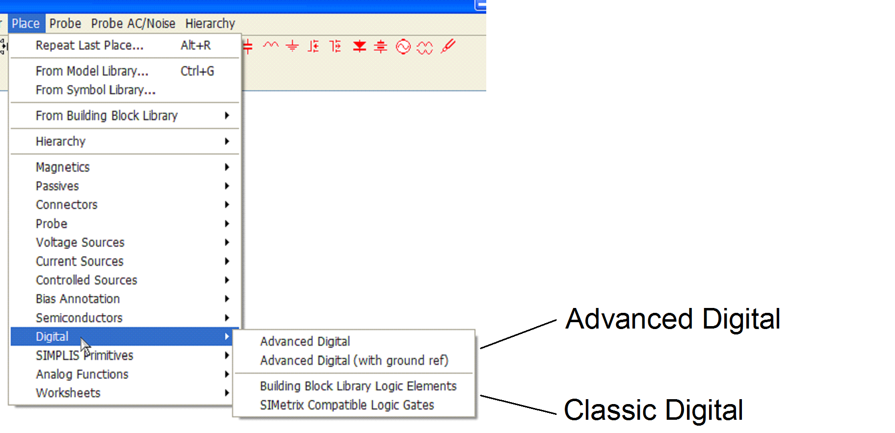
We refer to the new digital components as "Advanced Digital components" while referring to the traditional digital models in SIMPLIS as the "classic digital components." Beginning with SIMPLIS v5.6 , both classic and Advanced Digital components are supported and they are both available for placement on the schematic through a reorganized set of menus in the schematic editor.
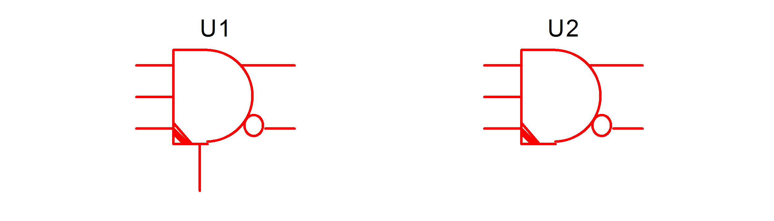
All Advanced Digital components have four slanted stripes in the lower left-hand corner of the symbol. For example, a 3-input AND gate will look like one of the following, where U1 has a ground-reference pin and U2 does not:
Classic Components
A component is considered a classic component if it meets all of the following requirements:
- It is NOT an Advanced Digital component.
- It is NOT a probe that measures voltage. For example, the regular voltage probe, the bus voltage probe, and the Bode plot probe are all probes that measure voltages.
- It is NOT a fixed pin current probe.
Similarities Between Classic and Advanced Digital Components
- Both classic digital components and Advanced Digital components employ similar analog parameters for modeling the input behavior. Typically, each input pin is modeled by an analog-to-digital interface bridge composed of a resistor RIN. Each input pin is modeled by a logic state of 0 or 1, depending on the value of the input voltage as compared to the threshold voltage TH and the hysteretic-window width HYSTWD.
- Both classic and Advanced Digital components employ similar analog parameters for modeling the output behavior. Typically, each output is modeled by a digital-to-analog interface bridge that is a composed of a resistor ROUT in series with a voltage source. The voltage source will have a value of VOL or VOH, depending on the logic output state of that output pin.
- Both classic and Advanced Digital components support devices with or without the ground reference pins, with a few minor exceptions.
- Both classic and Advanced Digital components model the switching of the outputs with zero rise time and zero fall time.
Differences between Classic and Advanced Digital Components
- While Advanced Digital components support analog parameters for modeling the input or output behavior, an A-to-D or D-to-A interface bridge is introduced if and only if the particular input or output pin is connected to a classic component. If an input or output pin of an Advanced Digital component is connected only to other Advanced Digital components, the probing of such a node will produce a waveform of logic values of 0, 1, or 0.5 (for an indeterminate logic value) versus time and it will be plotted as digital data in the upper portion of the waveform display tool. If you try to random probe the pin current of such a pin, the result will be a constant current of zero amperes since there is no analog circuitry to model the input or output behavior of such a pin. That is, if an input or output pin of an Advanced Digital component is connected only to other Advanced Digital components, the input associated with such an input or output pin exists only in the logical space and not in the analog space.
- For an Advanced Digital component, the ground reference pin MUST exist if at least one of the input pins or one of the output pins is connected to a classic component. When all of the input pins and all of the output pins of an Advanced Digital component are connected only to other Advanced Digital components, the ground reference pin is optional. Its presence or absence will not impact the simulation results.
- For a classic digital component without ground reference pin, each output produces an analog voltage through its Thevenin equivalent output with respect to the ground node in the schematic.
- While the delay parameter is optional and has a default value of 0.0 in the classic digital components, the delay parameters in the Advanced Digital components are mandatory and they are not allowed to be equal to 0.0.
- The classic digital components employ the "transport" delay model, which means for simple logic gates any glitches in the inputs are passed along to the output(s) after the defined delay. The Advanced Digital components employ the "inertial" delay model and glitches in the inputs that are shorter than the output-delay parameter are absorbed by the digital component and are not passed along to the output(s).
Strategies for Deploying the new Advanced Digital Components
The key to an efficient simulation using new SIMPLIS Advanced Digital components is to achieve the optimum balance between taking maximum advantage of the faster simulation times for Advanced Digital components while minimizing unnecessary interaction between new Advanced Digital components and the rest of the classic components in the SIMPLIS schematic.This can be accomplished using the following guidelines:
- Isolate Advanced Digital components as much as possible and try to locally minimize the number of I/O pins that are connected to classic components.
-
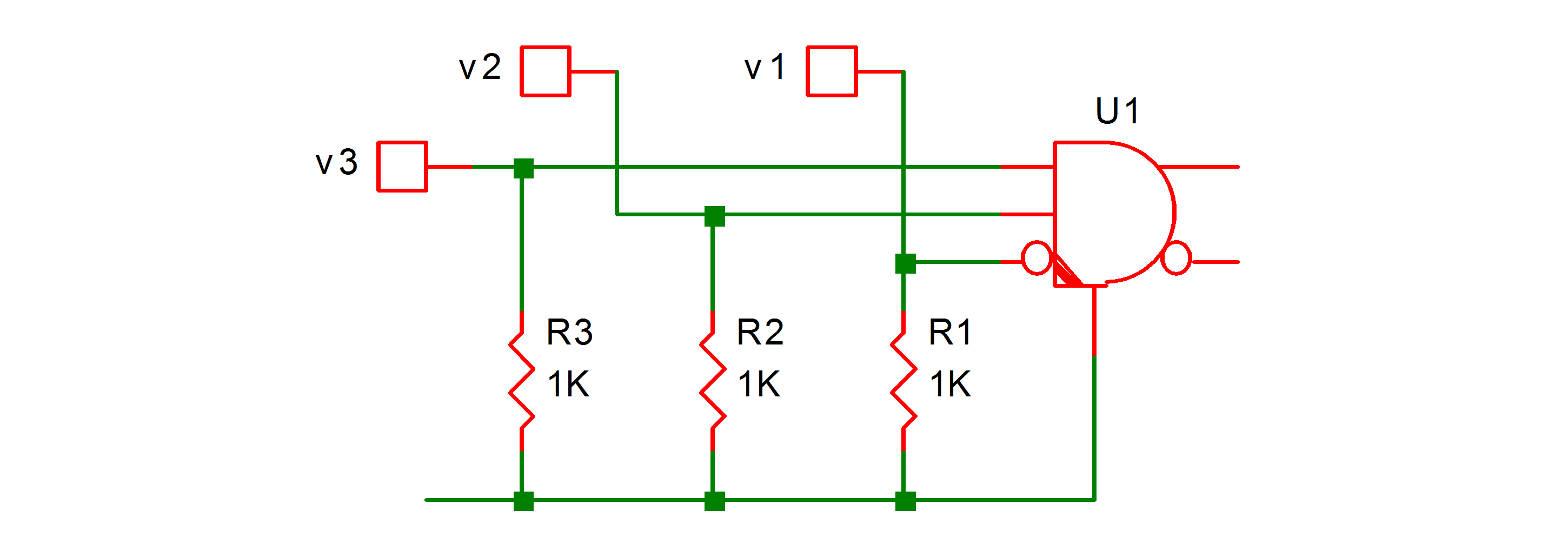
If most or all inputs to a simple logic gate are required to be connected to classic components, the simulation will run faster if a classic digital component is used as a front-end to drive a buffer from the Advanced Digital component library. For example, if all inputs to a three-input AND-gate are connected to classic analog components, a valid option is to have an Advanced Digital 3-input AND gate to sense the three analog inputs directly:
 However, for a more efficient and faster simulation, you should re-arrange the circuit and use a classic 3-input AND gate from the building-block library as the front-end to drive an Advanced Digital buffer. This approach is faster because the classic simulation engine only interrupts the Advanced Digital simulation when the logic state of the output of U2 changes, whereas, in the former case the classic simulation engine has to interrupt the Advanced Digital simulation any time one of the three inputs of the AND-gate changes logic state.
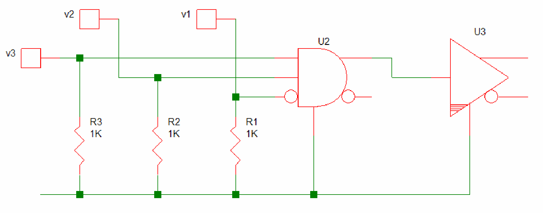 In this example, you should assign zero delay to U2, the classic 3-input AND gate and the non-zero delay to U3, the Advanced Digital buffer.
- For an Advanced Digital component that has at least one I/O pin connected to an analog node, you must use the version that includes the ground reference pin.
- For an Advanced Digital component whose I/O pins are all connected only to other Advanced Digital components, either the version that includes the ground reference pin or the version that does not include the reference pin can be used. The choice is up to the preference of the user and will not impact the simulation results.
A Simple DEMO Circuit
There is an example circuit supplied at Examples\SIMPLIS\Digital_PWM\SyncBuck_Digital_PWM.sxsch. This is a hierarchical schematic representing a simple synchronous buck converter controlled by a PWM controller employing PID compensation. This PWM controller is entirely made up from new Advanced Digital components.
| ◄ Synopsis of Small-Signal AC Analysis | Advanced Digital Component Reference ▶ |