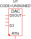
Digital to Analog Converter (Non-Clocked)
The Digital to Analog Converter models a generic DAC.
- The DAC output continuously responds to the digital signals applied at the inputs.
- The output voltage follows the input digital word with a propagation delay set by the Output Delay.
- The output voltage is scaled by the Range parameter and offset by the Offset parameter.
In this topic:
| Model Name: | Digital to Analog Converter | |||
| Simulator: | This device is compatible with the SIMPLIS simulator. | |||
| Parts Selector Menu Location: | ||||
| Symbol Library: | None - the symbol is automatically generated when placed or edited. | |||
| Model Library: | None - the model is automatically generated when the simulation is run. | |||
| Subcircuit Name: | SIMPLIS_DIGI1_D_D2A_CONVERTER_Y | |||
| Symbol: |
|
|||
| Multiple Selections: | Only one device at a time can be edited. | |||
Editing the Digital to Analog Converter
To configure the Digital to Analog Converter, follow these steps:
- Double click the symbol on the schematic to open the editing dialog to the Parameters tab.
- Make the appropriate changes to the fields described in the table below the image.
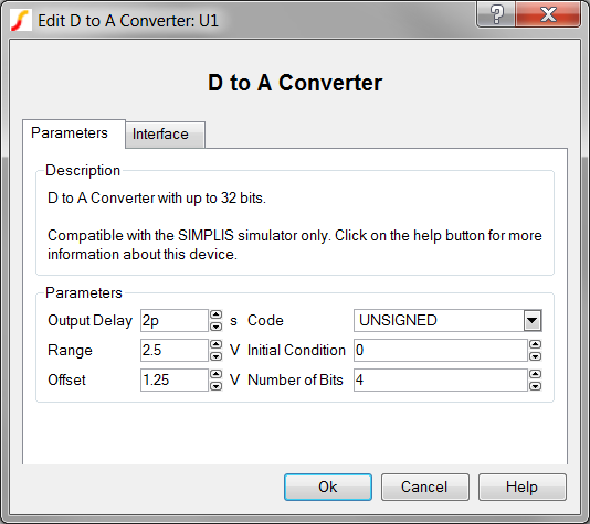
| Label | Parameter Description |
| Output Delay | Delay from when the input state changes until the output changes |
| Range | Analog output voltage range |
| Offset | Midpoint of analog output voltage range |
| Code | Encoding scheme for binary inputs of the DAC |
| Initial Condition | Initial condition of the DAC output at time=0 |
| Number of Bits | Number of input bits for this Digital to Analog Converter |
To define the parameters for the interface between this digital component and each analog component connected directly to an input or output pin, follow these steps:
- From the Edit Digital to Analog Converter dialog box, click on the Interface tab.
- Make the appropriate changes to the fields described in the table below the image.
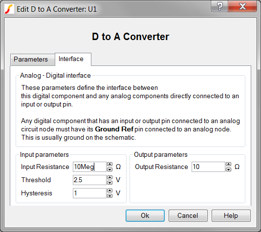
| Label | Parameter Description | |||||||
| Input Resistance | Input resistance of each DAC input pin | |||||||
| Hysteresis, Threshold | 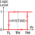 |
Hysteresis and
Threshold of the inputs. The hysteretic-window width, HYSTWD
is centered around Threshold (TH) voltage. To
determine the actual threshold ( TL , THI ),
substitute Threshold (TH) and Hysteresis
(HYSTWD) in each of the following formulas:
|
||||||
| Output Resistance | Output resistance of each DAC output pin | |||||||
Examples
The test circuit used to generate the waveform examples in the next section can be downloaded here: simplis_062_dac_example.sxsch.
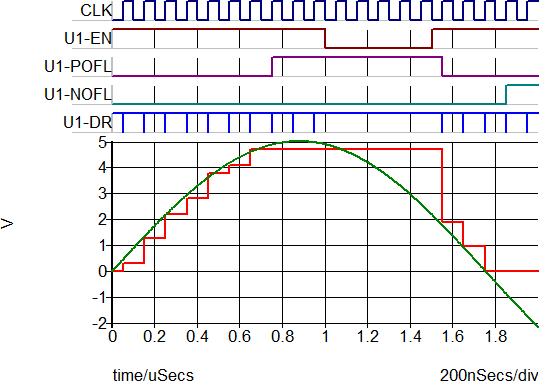
Waveforms
Subcircuit Parameters
Because the Digital to Analog Converter model is generated by a template script when the simulation is executed, a hand-coded model cannot be inserted into a netlist. The template script for this device is simplis_make_a2d_model.sxscr, which licensed users can download as part of a zip archive of all built-in scripts.
To download the zip archive, follow these steps:
- Click http://www.simetrix.co.uk/simetrix80/scripts.zip to download the script archive.
- Enter the user name and password you received with your license file.
The following parameter table defines the parameters used in this model.
| Parameter Name | Label | Data Type | Range | Units | Parameter Description | |||||||
| CODE | Code | String |
|
none | Encoding scheme for binary inputs of the DAC | |||||||
| HYSTWD, TH |
Hysteresis, Threshold |
Number | min: 1f | V | |
Hysteresis and Threshold of
the inputs. The hysteretic-window width, HYSTWD is centered around
Threshold (TH) voltage. To determine the actual threshold (
TL , THI ), substitute Threshold (TH) and
Hysteresis (HYSTWD) in each of the following formulas:
|
||||||
| IC | Initial Condition | Number |
|
none | Initial condition of the DAC output at time=0 | |||||||
| NUMBITS | Number of Bits | Integer | none | Number of input bits for this Digital to Analog Converter | ||||||||
| OUTPUT_OFFSET | Offset | Number | any | V | Midpoint of analog output voltage range | |||||||
| OUTPUT_RANGE | Range | Number | any | V | Analog output voltage range | |||||||
| OUT_DELAY | Output Delay | Number | 1f to 1024 | s | Delay from when the input state changes until the output changes | |||||||
| RIN | Input Resistance | Number | min: 100 | Ω | Input resistance of each DAC input pin | |||||||
| ROUT | Output Resistance | Number | min: 1m | Ω | Output resistance of each DAC output pin | |||||||