Switched Voltage-Controlled Voltage Source
The Switched Voltage-Controlled Voltage Source (VCVS) models the passing of an analog voltage from input to output with unity gain. The block uses an ON/OFF control where:
- VOUT voltage = VIN voltage when the control signal is in the ON state.
- VOUT voltage = 0 when the control signal is in the OFF state.
In the discussion here, the VIN voltage, the input voltage, or the input signal refers to the voltage of the VIN pin with respect to the voltage of the RTN pin, whereas the CNTL voltage, the control voltage, or the control signal refers to the voltage of the CNTL pin with respect to the voltage of the RTN pin. Similarly, the VOUT voltage, the output voltage, or the output signal refers to the voltage of the VOUT pin with respect to the voltage of the RTN pin.
Furthermore, the VIN and CNTL pins are voltage sensing inputs and they will draw zero currents. The VOUT pin and the RTN pin together form a voltage source, with the VOUT voltage either tracking the VIN voltage or it is clamped to zero. The VOUT pin will produce or draw current to maintain the output voltage and the RTN pin provides the return path for such a current.
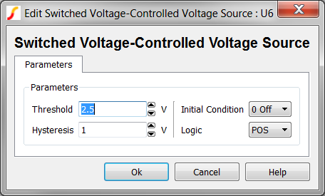
The Logic parameter sets the control state logic. The two choices are:
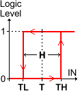
- POS – The control signal is considered to be in the ON state when the CNTL voltage is greater than Threshold +1/2 Hysteresis.
- NEG - The control signal is considered to be in the ON state when the CNTL voltage is less than Threshold – 1/2 Hysteresis.
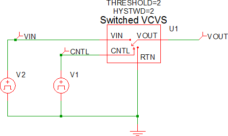
Most users implement this function with two simple switches connected in a totem-pole configuration where VIN is the input voltage and VOUT is the output voltage.
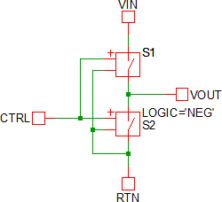
Because the SIMPLIS simple switches S1 and S2 have finite ON and OFF resistances, the totem-control configuration will always have numeric inaccuracies. These inaccuracies are caused by the inherent resistive divider network formed by the switch resistances.
In contrast to the totem-pole switch circuit, this block was designed to eliminate the numeric inaccuracies caused by the voltage divider. You should always use this block instead of a totem-pole switch configuration since this block does not exhibit the numeric inaccuracy inherent to the totem-pole switch configuration.
In this topic:
| Model Name: | Switched Voltage-Controlled Voltage Source | |
| Simulator: | This device is compatible with the SIMPLIS simulator. | |
| Parts Selector Menu Location: |
|
|
| Symbol Library: | simplis_analog_functions.sxslb | |
| Model File: | simplis_analog_functions.lb | |
| Subcircuit Name: | SIMPLIS_SWITCH_VCVS_BB | |
| Symbols: | 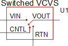
|
|
| Multiple Selections: | Multiple devices can be selected and edited simultaneously. | |
Previous Version Compatibility
This symbol was introduced with version 8.0; however, the model and supporting files are available in version 7.20 as well. In versions prior to 7.20, the schematic will simulate, but you will not be able to edit the parameters with the dialog pictured in this topic.
For a version of the Switched VCVS compatible with versions prior to version 7.20, see the parts selector entry:
Symbol Migration
Symbols placed on schematics in previous versions of SIMetrix/SIMPLIS can be automatically migrated to use the new symbols. The schematic tools menu will invoke a routine which migrates the existing symbols to the new symbols. As this action makes substantial changes to the schematic, it is recommended that you save a backup copy of the schematic first.
I/O Table
The following table describes the pins on the Switched VCVS symbol.
| Pin_Name | I/O | Function | Description |
| CNTL | I | On/Off control voltage | The threshold voltage, hysteresis, and logic of the control voltage are set in the input dialog box described in Editing_the_Switched_VCVS. |
| VIN | I | Input voltage for VCVS | The input voltage for the VCVS |
| RTN | Circuit return for this VCVS | The ground reference for this circuit | |
| VOUT | O | Output Voltage for VCVS | VOUT voltage = VIN voltage when the CNTL signal is in the ON state. VOUT voltage = 0 when the CNTL signal is in the OFF state. The VIN and VOUT voltages are all defined with respect to the voltage at the RTN pin. The initial condition can be set to either ON or OFF. |
Editing the Switched VCVS
To configure the Switched VCVS, follow these steps:
- Double click the symbol on the schematic to open the editing dialog.
- Make the appropriate changes to the fields described in the table below the image.
| Label | Parameter Description | |||||||
| Threshold Hysteresis |
|
The
Threshold (T) and Hysteresis (H) of the VCVS.
To determine the low-to-high threshold (TH) and the high-to-low
threshold (TL), substitute Threshold (T) and
Hysteresis (H) in each of the following formulas :
|
||||||
| Initial Condition | Initial condition of the CNTL signal; default is 0 Off. | |||||||
| Logic | The logic of the CNTL signal, which can be set to positive or negative; default is POS. | |||||||
Example
The test circuit used to generate the waveform examples in the next section can be downloaded here: simplis_071_switched_vcvs.sxsch.
Waveforms
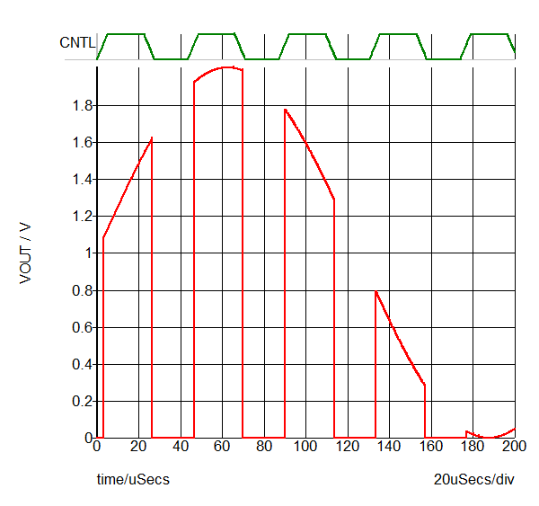
The waveform below is the test circuit showing a sinusoidal VIN waveform and an asynchronous CNTL waveform.
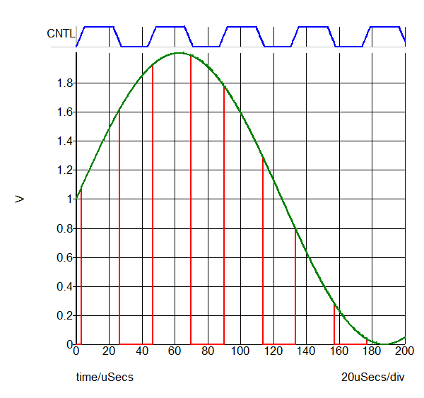
The following waveform is for the test circuit with VIN hidden.