SystemDesigner Shift Operation
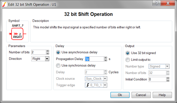
The SystemDesigner Shift devices model a left or right shift operation. If the Direction is Left, the output is multiplied by 2 Number of bits . If the Direction is Right, the output is divided by 2 Number of bits . For integer simulations, the shift right operation truncates the remainder of the division; for example, if the number 7 is shifted right one place, the result is 3. The same operation in a floating-point simulation results in 3.5. The Shift Operation output is a SystemDesigner bus with a 32-bit signed-integer or floating-point result. From the Output parameter box, you can limit the resulting output to either signed or unsigned numbers with fewer than 32 bits.
The propagation delay can be defined as a fixed time, as asynchronous to any clock, or as a synchronous delay where the delay is a number of SystemDesigner -clocks cycles. In this release of SystemDesigner , the synchronous delay is supported only for integer-sampled data simulations.
In this topic:
| Model Name: | SystemDesigner Shift Operation | |||||
| Simulator: | This device is compatible with the SIMPLIS simulator. | |||||
| Parts Selector Menu Location: | SystemDesigner Functions (max. 32 bit) | |||||
| Symbol Library: | SIMPLIS_SystemDesigner.sxslb | |||||
| Model Library: | SIMPLIS_SystemDesigner.lb | |||||
| Subcircuit Names: |
|
|||||
| Symbols: |
|
|||||
| Multiple Selections: | Only one device at a time can be edited. | |||||


Editing the SystemDesigner Shift Operation
To configure the SystemDesigner Shift Operation, follow these steps:
- Double click the symbol on the schematic to open the editing dialog to the Parameters tab.
- Make the appropriate changes to the fields described in the table below the image.
| Label | Parameter Description |
| Number of bits | The number of bit to shift the output |
| Direction | The shift direction.
|
| Use asynchronous delay | Implements a combinatorial model where the output voltage changes in response to the input voltage change after a propagation delay. |
| Propagation delay | The propagation delay from an input change to an output change in seconds. This parameter is used only in models with Asynchronous delay. |
| Use synchronous delay | In response to an input voltage change, the output voltage changes after a designated number of clock cycles. |
| Delay | The propagation delay from an input change to an output change in number of clock cycles. The output will not change until the number of clock cycles has been reached. The output will then change state only on the selected Clock source edges specified by Trigger edge . This parameter is used only in models with Synchronous delay. |
| Clock source | Specifies the global clock used for the Shift Operation. The Clock can be set up using the SystemDesigner->Edit SystemDesigner Clocks... menu item or by placing a Start of Conversion Breakin. |
| Trigger edge | Sets the Shift Operation output to change on specific edges of the Clock:
|
Examples
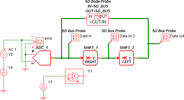
A Shift Left and Right circuit using both shift operations can be downloaded here: simplis_121_systemdesigner_shift_example.sxsch. In order to simulate this design, follow these steps:
- If you currently have a dialog box open in SIMetrix/SIMPLIS, cancel that dialog box so that the example can open in SIMetrix/SIMPLIS.
- Unzip the archive to a location on your computer.
- To open the schematic, double click the .sxsch file or drag that file into the SIMetrix/SIMPLIS Command Shell.
Waveforms
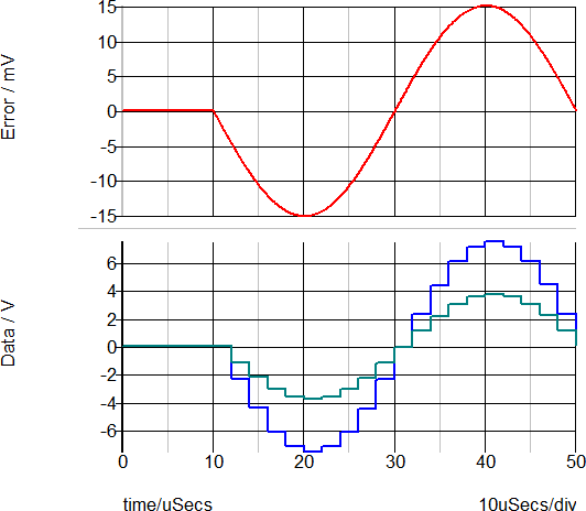
The circuit example below uses an ADC to generate the input to the Shift Right operation, SHIFT_1. The Shift Right operation divides this bus by 2, causing truncation when the simulation is run in the integer-sampled data mode with the input bus equal to 7. The Shift Left operation effectively gains the output of the Shift Right Operation, restoring the signal to the same amplitude as the input, excluding truncation errors.
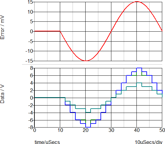
During floating-point simulations, the Shift operation "perfectly" divides the input signal, producing a double-precision floating-point output.
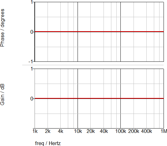
The AC transfer function for the Shift Operation is shown below. As expected, the gain is 0dB with no phase change.