Signal Level of a Node
As far as the SIMPLIS simulator is concerned, each node in a schematic can be classified as either an analog node or a digital node. By default, a node is an analog node. But if a node is connected to one or more digital devices and it is not connected to any analog components, then this node is considered a digital node.
The SIMPLIS classic digital devices, which can be identified by the lack of additional lines on the lower left corner of the symbol, are considered analog and not digital components for the purpose of this discussion. The inline current probes are also considered analog components. Voltage probes and bus probes, however, are not considered analog components for the purpose of this discussion. Hence, the voltage probes or bus probes would not be included in determining whether a node is an analog node or a digital node.
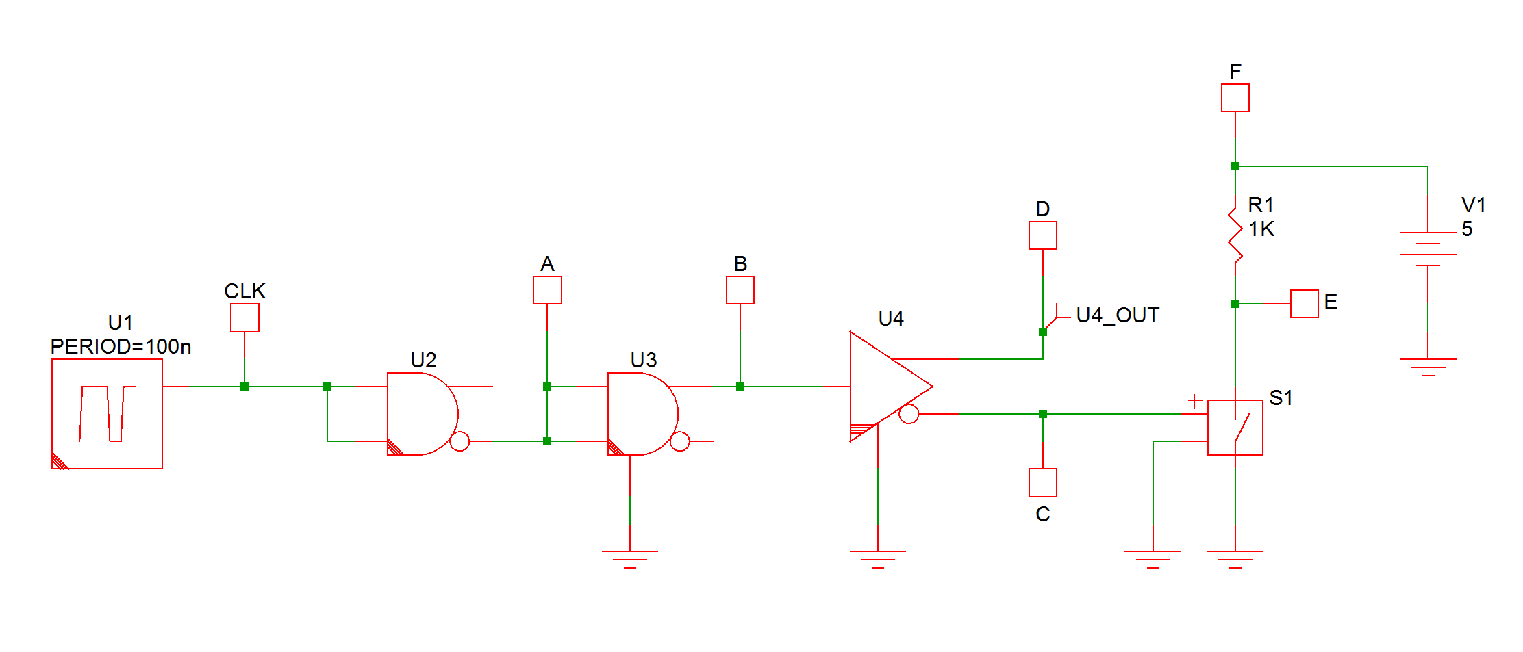
The following circuit example is intended to help you better understand the difference between an analog node and a digital node. Nodes CLK, A, B, and D are all considered digital nodes. Nodes C, E, and F are considered analog nodes. The fact that the AND gate U3 has a ground reference does not imply its input and output pins are connected to analog nodes. It only means that it is acceptable for its pins to touch analog components. Since there are no analog components connected to nodes A and B, these two nodes are considered digital nodes. Node C is an analog node since it is connected to a voltage-controlled switch, which is an analog component. Node D is connected to one digital device, U4, and a voltage probe, and no analog components. Hence, node D is considered a digital node. Nodes E and F are analog nodes since they do not touch any digital devices at all.
This example circuit can be downloaded here: simplis_analog_and_digital_nodes_example.sxsch
If a node is considered a digital node, then its signal level is represented by the logic level. If a node is an analog node, then its signal level is represented by the voltage at this node. This section describes how the SIMPLIS simulator arrives at the signal level of a node that is connected to at least one pin of a digital device. Notice that this node could be an analog node or a digital node, depending on whether it is also connected to pins of analog components. Understanding how the SIMPLIS simulator arrives at the signal level of such a node helps interpreting the waveforms displayed in the waveform viewer and helps understanding how the SIMPLIS simulator determines the logic level of each input pin of a digital device.
Logic Levels
The digital simulator in SIMPLIS supports three different logic levels:
| Logic Level | Value |
| LOW | 0 |
| HIGH | 1 |
| UNKNOWN | X |
The logic level of UNKNOWN means it could not be determined whether it is LOW or HIGH.
Output Strengths
The digital simulator in SIMPLIS supports three different output strengths. In descending order of strengths, they are:
| Output Strength | Value |
| STRONG | S |
| RESISTIVE | R |
| HIGH-IMPEDANCE | Z |
The output strength is associated with the output pins of the digital devices and the concept of output strength is useful for determining the logic level of a node that is connected to more than one output pin from one or more digital devices.
The output pins of all digital devices in SIMPLIS, except for the tri-state buffers and pull resistors, are assigned STRONG output strengths. The output pins of a tri-state buffer are set to have STRONG output strengths when it is enabled but set to HIGH-IMPEDANCE output strengths when it is disabled. The output pins of a pull resistor are always set to RESISTIVE output strengths.
Output State of an Output Pin
At any given instant, each output pin of a SIMPLIS digital device assumes an output state that is made up of two components: the logic level and the output strength. Both the logic level and the output strength are set according to the current logic levels of its input pins, any existing state information, and the functionality of the device.
For example, if the input pin of a digital buffer has a logic level of UNKNOWN (X), then the output state of the output pin of this device will be XS, with X representing the UNKNOWN logic level and S to represent the strong output strength.
Logic Level of a Digital Node
When a digital node is only connected to input pins of digital devices but it is not connected to the output pins of any digital devices, the logic level of this node is set to UNKNOWN (X). Since this a digital node, there are obviously no analog components attached to it either. Hence, the logic level of this node is unknown as nothing in the schematic is driving this node.
When a digital node is connected to one output pin of a digital device and zero or more input pins of digital devices, the logic level of this node is set to the logic level of that particular output pin.
When a digital node is connected to more than one output pin from one or more digital devices and zero or more input pins of digital devices, the logic level of this node is resolved through the following rules:
- Comparing the output strengths of all output pins connected to this node, those output pins with the highest output strength are considered dominating output pins.
- If there is only one dominating output pin, the logic level of this node is set to the logic level of this dominating output pin.
- If there is more than one dominating output pin, the logic level of this node is set to the logic level of these dominating output pins if the logic levels of these output pins are identical. On the other hand, if the logic levels of the dominating output pins are not identical, then the logic level of this node is set to UNKNOWN (X).
When a voltage probe is attached to a digital node, the waveform viewer will display 0, 0.5, or 1 for this node if the logic level of this node is equal to LOW (0), UNKNOWN (X), and HIGH (1), respectively. This is true whether this waveform is displayed on an analog or digital vertical axis.
Voltage of an Analog Node
When a node is connected to at least one pin of a digital device and it is also connected to one or more analog components, then this node is considered an analog level. In this case, all relevant pins from digital devices connected to this node are represented by their "analog interfaces." The following figure illustrates such representations:
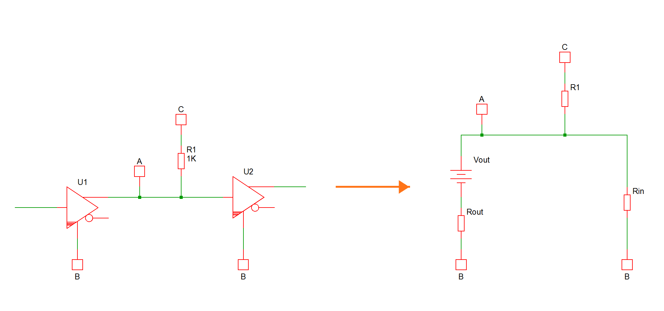
This simple circuit could be part of a much more elaborate schematic with many other components. Obviously, node A is an analog node due to the connection to the resistor R1. On the analog side of SIMPLIS, the output of U1 here is represented by a series connection of a resistor Rout with a DC voltage source Vout. On the analog side of SIMPLIS, the input of U2 is presented by a resistor Rin to represent the input resistance.
The input resistance of the digital device does not change during the simulation and it is set to the "Input Resistance" specified in the "Interface" tab of the Edit dialog of the device.
The voltage of Vout is set according to the logic level of the corresponding output pin during the simulation. It will be set to "Output Low Level" and "Output High Level" if the logic level of the output pin is equal to LOW (0), or HIGH (1), respectively. You can find "Output Low Level" and "Output High Level" in the "Interface" tab of the Edit dialog of the device. If the logic level of the output pin is equal to UNKNOWN (X), the voltage of Vout is set to the average value between the "Output Low Level" and the "Output High level."
The resistance of Rout is set according to the output strength of the output pin. For an output pin that have a fixed output strength, the resistance of Rout will be set to the "Output Resistance" or "Resistance" defined in the "Interface" tab of the Edit dialog of the device. For an output pin that exhibits more than one output strength, the resistance of this resistor will be set according to the output strength of the output pin and the corresponding output resistance parameters defined in the "Interface" tab of the Edit dialog of the device.
To arrive at the voltage of an analog node which is connected to at least one pin of a digital device, SIMPLIS replaces the relevant inputs/outputs of the connected digital devices by their analog interfaces. Taking into consideration ALL other analog components connected to this node, the voltage of this node is solved. If this node is connected to any input pin of a digital device, the logic level of this input pin is then computed according to the "Input Parameters" defined in the "Interface" tab of the Edit dialog for this device.
If input pins from more than one digital device are connected to the same analog node, it is possible that, at some time durations, these input pins are set to different logic levels from each other despite the fact that they are connected to the same analog node. This could happen when the "Threshold" and "Hysteresis" input parameters of the different concerned digital devices are not identical.
When a voltage probe is attached to an analog node which is connected to at least one pin of a digital device, the waveform viewer will display the voltage of this node, similar to how the voltage of a node in an analog circuit is displayed.