SystemDesigner Clocks
SystemDesignerdistributes global clocks to every SystemDesigner component. Although most designs require only a single system clock, having lower or higher frequency clocks may be useful in some cases.
You can define up to eight clocks (SysCLK plus User1 through User7) as shown in the dialog
and explained in the table below.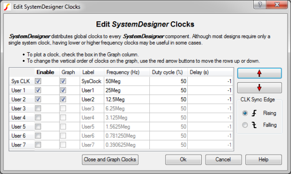
| Column | Edit control type | Definition |
| Enable | CheckBox | Enables each clock. Disabled clocks are not included in the simulation. |
| Graph | CheckBox | If checked, the clock waveform appears in the graph viewer. Clocks need not be graphed to use on the schematic. |
| Label | String | The label assigned to the curve. The label cannot contain spaces. |
| Frequency (Hz) | String | The clock frequency in Hz. |
| Duty cycle (%) | String | The clock duty cycle in percent. |
| Delay (s) | String | The delay in seconds. If the delay is less than 0, each clock is given a delay = 0.5 times the highest frequency clock period. |
Defining SystemDesigner Clocks
To define and edit a SystemDesigner clock, follow these steps:
- From the menu bar in the schematic, select SystemDesigner | Edit SystemDesigner
Clocks. Result: The Edit SystemDesigner Clocks dialog appears.
- Check the box in the Enable column.
- To show the clock in the graph viewer, check the box in the Graph column.
- Add a unique name for the clock in the Label column.
- Change the frequency, duty cycle, and delay values as needed.
- To synchronize the rising or falling edges of all harmonically related clocks,
select either Rising or Falling from the CLK Sync Edge section in the
lower right corner of the dialog.
 Note: If the clocks are not harmonically related, only the first edge will be in sync.
Assigning the vertical order
Each system clock (SykCLK, User1 through User7) is assigned a vertical order string = clk n , where "n" is 0 through 7. To change the default order of the system clocks, follow these steps:
- In the Edit SystemDesigner Clocks dialog, select a row in the table.
- Use the red arrows to move the selected row up or down.
If you want to include probes in the graph viewer, you can assign a string to the probe in order to place it either above or below the system clocks. Since each system clock label begins with a c, use the following approach to define the placement of probes on the graph.
- To place probes above the system clocks, assign a Display order string that begins with a or b.
- To place probes below the system clocks, assign a Display order string that begins with the letters d through z.
To assign a Display order string to the SystemDesigner bus probe, follow these steps:
- Double click the SystemDesigner probe on your schematic.Result: The Edit SystemDesigner Bus Probe dialog appears as shown below with a blue box surrounding the area where you define the vertical order string.Note: The Plot Integer data as option must be set to Digital bus in order to display the probe on the digital axis with the other global clocks.
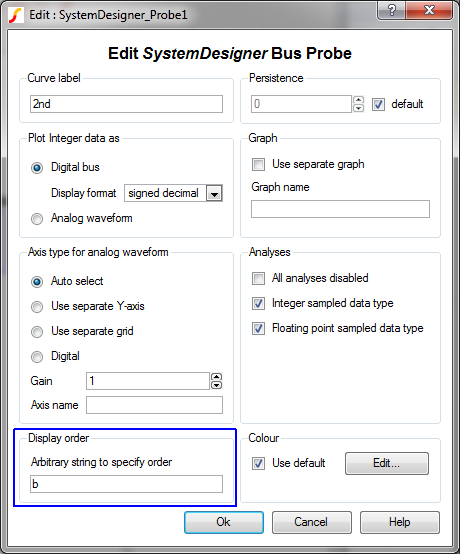
- In the Display ordertext box, do one of the following:
- If you want the probe to appear above the system clocks on the graph, type
aor b or a string starting with one of those letters.
or
- If you want the probe to appear below the system clocks on the graph, type a letter or string starting with a letter between dand z.
- If you want the probe to appear above the system clocks on the graph, type
aor b or a string starting with one of those letters.
To define the order of other probes, double click the probe and set the Display order in the same way as you set the SystemDesigner bus probe. For the Display order to take effect, the other probes must be output to the digital axis.
Previewing the clocks
From the Edit SystemDesigner Clocks dialog, you use the Close and Graph Clocks button to run a simulation on the clocks defined in that dialog. No components from the currently selected schematic will be included in this simulation.
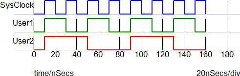
For example, the following dialog has three system clocks defined:
To save the clock information and simulate those three clocks, click Close and Graph Clocks.
Exposing a global clock at any schematic level
If you want to expose a global clock to a schematic, a special symbol, the SystemDesigner Global Clock Breakout, is available to expose the global clock on a symbol pin that can be wired to any analog or digital component on the schematic, such as the one below.
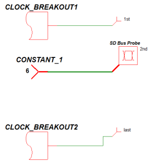
In clocks_example.sxsch, two global clocks have been exposed through the SystemDesigner Global Clock Breakout devices, and connected to regular voltage probes. A SystemDesigner Constant has also been placed on the schematic, and a SystemDesigner bus probe has been added to plot the constant value. Each probe has been assigned a Display order string of a, b, or z.
- The probe labeled 1st has the vertical Display order set to a.
- The probe labeled 2ndhas the vertical Display order set to b.
- The probe labeled last has the vertical order z.
The resulting graphs show the probes in the correct vertical order.
- The global clocks, SysClock, User1 and User2 have Display order strings of clk0, clk1, and clk2 respectively. These strings are automatically assigned by the program.
- The waveforms 1st and 2nd, appear above the global clocks because these probes have the Display order strings of a and b, respectively.
- The probe with the label last appears below the global clocks because the Display order string is z.
Digital waveforms are ordered alphabetically by the Display order string.
