SystemDesigner A-to-D Converter
The SystemDesigner A-to-D Converter (ADC) models a generic sample/hold and quantizer. The input is a differential voltage; the output is a SystemDesigner bus with a 32-bit signed-integer or floating-point result. From the Output parameter box, you can limit the resulting output to either signed or unsigned numbers with fewer than 32 bits.
The ADC converts the analog input on a SystemDesigner -clock edge or on one of the Global Start-of-Conversion (SOC) signals. The SOC signals may be generated by the ePWM modules. Multiple ADCs can use the same clock or the SOC signal.
The propagation delay can be defined as a fixed time, as asynchronous to any clock, or as a synchronous delay where the delay is a number of SystemDesigner -clocks cycles. In this release of SystemDesigner , the synchronous delay is supported only for integer-sampled data simulations.
In this topic:
| Model Name: | SystemDesigner A-to-D Converter | |||
| Simulator: | This device is compatible with the SIMPLIS simulator. | |||
| Parts Selector Menu Location: | ||||
| Symbol Library: | SIMPLIS_SystemDesigner.sxslb | |||
| Model Library: | SIMPLIS_SystemDesigner.lb | |||
| Subcircuit Name: | SIMPLIS_SD_ADC_32 | |||
| Symbol: |
|
|||
| Multiple Selections: | Only one device at a time can be edited. | |||

Editing the SystemDesigner A-to-D Converter
To configure the SystemDesigner A-to-D Converter, follow these steps:
- Double click the symbol on the schematic to open the editing dialog to the Parameters tab.
- Make the appropriate changes to the fields described in the table below the image.
| Label | Parameter Description |
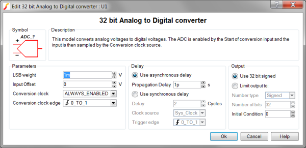
| LSB weight | The voltage amplitude which represents the least significant bit of the ADC |
| Input Offset | The input voltage which represents a zero output on the ADC |
| Conversion clock | The Conversion
clock samples and converts the analog input to a digital
output on every Conversion clock signal edge defined by
Conversion clock edge . Possible Conversion clock
sources include the global system clocks and the Start of
conversion signals generated by the ePWM blocks or Breakins:
|
| Conversion clock edge | Sets the sampling on
specific edges of the Conversion clock source :
|
| Use asynchronous delay | Implements a combinatorial model where the output voltage changes in response to the input voltage change after a propagation delay. |
| Propagation delay | The propagation delay from an input change to an output change in seconds. This parameter is used only in models with Asynchronous delay. |
| Use synchronous delay | In response to an input voltage change, the output voltage changes after a designated number of clock cycles. |
| Delay | The propagation delay from an input change to an output change in number of clock cycles. The output will not change until the number of clock cycles has been reached. The output will then change state only on the selected Clock source edges specified by Trigger edge . This parameter is used only in models with Synchronous delay. |
| Clock source | Specifies the global clock used for the ADC. The Clock can be set up using the SystemDesigner->Edit SystemDesigner Clocks... menu item or by placing a Start of Conversion Breakin. |
| Trigger edge | Sets the ADC output to change on specific edges of the Clock:
|
| Use 32 bit signed | The full 32-bit signed data is output. |
| Limit output to: | The output is limited to a Signed or Unsigned number with a designated number of bits. |
| Number type | The output will be limited to either a Signed or Unsigned number if Limit output to is selected.
This parameter is used only in models with Limit output to selected. |
| Number of bits | The limit on the output depends on the Number type parameter:
This parameter is used only in models with Limit output to selected. |
| Initial Condition | Initial condition of the output at time=0. Value is the output bus represented in decimal format. |
Examples
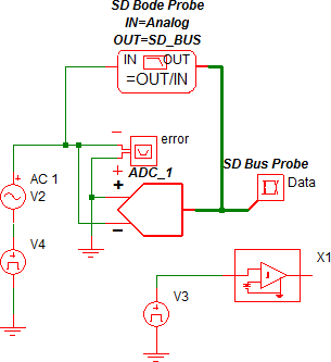
The ADC circuit used to generate the following waveforms can be downloaded here: simplis_119_systemdesigner_adc_example.sxsch. In order to simulate this design, follow these steps:
- If you currently have a dialog box open in SIMetrix/SIMPLIS, cancel that dialog box so that the example can open in SIMetrix/SIMPLIS.
- Unzip the archive to a location on your computer.
- To open the schematic, double click the .sxsch file or drag that file into the SIMetrix/SIMPLIS Command Shell.
A similar example using the DAC can be downloaded here: simplis_120_systemdesigner_dac_example.sxsch
Waveforms
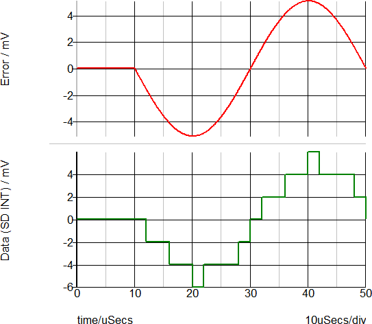
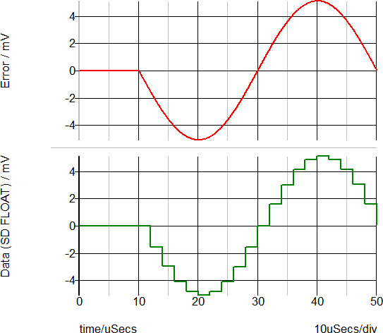
The Input voltage to the ADC is a sine wave with the following parameters:
- Amplitude = +/- 5.1mV
- Period = 40us
- Delay =10us.
During the delay time, the sine wave source has a value of zero volts.
During integer-sampled data simulations, the sine wave voltage is sampled by the ADC and quantized into BIN_SIZE amplitude values. The BIN_SIZE is set to 2mV with a variable in the F11 window of the schematic. The quantized amplitude of the data signal has a maximum value of 3 LSB counts. The output signal is probed with the SystemDesigner probe data.
For double-precision floating-point sampled-data simulations, the ADC behaves as a sample/hold and gains the result by 1/BIN_SIZE, which, with a BIN_SIZE of 2mV, is a gain of 500. The output of the ADC is, therefore a sampled-time analog voltage, but without amplitude quantization. The peak amplitude of the ADC is 5.1mV * 1/BIN_SIZE or 2.55V. Notice the difference between this output and the output for the integer-data simulation. In the integer simulation, the data signal takes on discrete amplitudes, whereas in the floating point simulation, the amplitudes are not quantized.
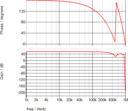
The AC transfer function for the adder is shown below. The DC gain is 54dB, (1/BIN_SIZE).